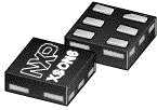

74AXP1G07GS - Low-power buffer with open-drain output
74AXP1G07GS是NXP公司的一款缓冲器/驱动器产品,74AXP1G07GS是Low-power buffer with open-drain output,本站介绍了74AXP1G07GS的封装应用图解、特点和优点、功能等,并给出了与74AXP1G07GS相关的NXP元器件型号供参考。
74AXP1G07GS - Low-power buffer with open-drain output - 缓冲器/驱动器 - 逻辑 - 恩智浦, LLC
产品描述
The 74AXP1G07 is a non-inverting buffer with open-drain output.
Schmitt-trigger action at the input makes the circuit tolerant of slower input rise andfall times.
This device ensures very low static and dynamic power consumption across the entireVCC range from 0.7 V to 2.75 V. It is fully specified for partial powerdown applications using IOFF. The IOFF circuitry disables theoutput, preventing the potentially damaging backflow current through the device when itis powered down.
产品特性和优势
- Wide supply voltage range from 0.7 V to 2.75 V
- Low input capacitance; CI = 0.5 pF (typical)
- Low output capacitance; CO = 0.7 pF (typical)
- Low dynamic power consumption; CPD = 1.0 pF at VCC = 1.2 V(typical)
- Low static power consumption; ICC = 0.6 μA (85 °C maximum)
- High noise immunity
- Complies with JEDEC standard:
- JESD8-12A.01 (1.1 V to 1.3 V)
- JESD8-11A.01 (1.4 V to 1.6 V)
- JESD8-7A (1.65 V to 1.95 V)
- JESD8-5A.01 (2.3 V to 2.7 V)
- ESD protection:
- HBM ANSI/ESDA/JEDEC JS-001 Class 2 exceeds 2 kV
- CDM JESD22-C101E exceeds 1000 V
- Latch-up performance exceeds 100 mA per JESD 78 Class II
- Inputs accept voltages up to 2.75 V
- Low noise overshoot and undershoot < 10 % of VCC
- IOFF circuitry provides partial Power-down mode operation
- Multiple package options
- Specified from -40 °C to +85 °C
下面可能是您感兴趣的NXP公司缓冲器/驱动器元器件


NXP公司产品现货专家,订购NXP公司产品不限最低起订量,NXP芯片大陆现货即时发货,香港库存3-5天发货,海外库存7-10天发货
寻找全球NXP代理商现货货源 - NXP公司(恩智浦)电子元件在线订购


