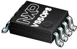

74AXP1T57DC是NXP公司的一款电平转换器产品,74AXP1T57DC是Dual supply configurable multiple function gate,本站介绍了74AXP1T57DC的封装应用图解、特点和优点、功能等,并给出了与74AXP1T57DC相关的NXP元器件型号供参考。
74AXP1T57DC - Dual supply configurable multiple function gate - 电平转换器 - 逻辑 - 恩智浦, LLC
The 74AXP1T57 is a dual supply configurable multiple function gate with Schmitt-trigger inputs.It features three inputs (A, B and C), an output (Y) and dual supply pins(VCCI and VCCO). The inputs are referenced to VCCIand the output is referenced to VCCO. All inputs can be connected directly toVCCI or GND. VCCI can be supplied at any voltage between 0.7 Vand 2.75 V and VCCO can be supplied at any voltage between 1.2 V and 5.5 V.This feature allows voltage level translation. The 74AXP1T57 can be configured as any ofthe following logic functions AND, OR, NAND, NOR, XNOR, inverter and buffer.
This device ensures very low static and dynamic power consumption across the entiresupply range and is fully specified for partial power down applications usingIOFF. The IOFF circuitry disables the output, preventing thepotentially damaging backflow current through the device when it is powered down.
- Wide supply voltage range:
- VCCI: 0.7 V to 2.75 V
- VCCO: 1.2 V to 5.5 V
- Low input capacitance; CI = 0.6 pF (typical)
- Low output capacitance; CO = 1.8 pF (typical)
- Low dynamic power consumption; CPD = 0.6 pF at VCCI = 1.2 V(typical)
- Low dynamic power consumption; CPD = 7.1 pF at VCCO = 3.3 V(typical)
- Low static power consumption; ICCI = 0.5 μA (85 °C maximum)
- Low static power consumption; ICCO = 1.8 μA (85 °C maximum)
- High noise immunity
- Complies with JEDEC standard:
- JESD8-12A.01 (1.1 V to 1.3 V; A, B, C inputs)
- JESD8-11A.01 (1.4 V to 1.6 V)
- JESD8-7A (1.65 V to 1.95 V)
- JESD8-5A.01 (2.3 V to 2.7 V)
- JESD8-C (2.7 V to 3.6 V; Y output)
- JESD12-6 (4.5 V to 5.5 V; Y output)
- ESD protection:
- HBM ANSI/ESDA/JEDEC JS-001 Class 2 exceeds 2 kV
- CDM JESD22-C101E exceeds 1000 V
- Latch-up performance exceeds 100 mA per JESD78D Class II
- Inputs accept voltages up to 2.75 V
- Low noise overshoot and undershoot < 10 % of VCCO
- IOFF circuitry provides partial power-down mode operation
- Multiple package options
- Specified from -40 °C to +85 °C


