


PCA9617ADP是NXP公司的一款I²C增强快速模式产品,PCA9617ADP是Level translating Fm+ I2C-bus repeater,本站介绍了PCA9617ADP的封装应用图解、特点和优点、功能等,并给出了与PCA9617ADP相关的NXP元器件型号供参考。
PCA9617ADP - Level translating Fm+ I2C-bus repeater - I²C增强快速模式 - I²C - 恩智浦, LLC
The PCA9617A is a CMOS integrated circuit that provides level shifting between lowvoltage (0.8 V to 5.5 V) and higher voltage (2.2 V to 5.5 V) Fast-mode Plus (Fm+) I2C-busor SMBus applications. While retaining all the operating modes and features of theI2C-bus system during the level shifts, it also permits extension of the I2C-bus by providingbidirectional buffering for both the data (SDA) and the clock (SCL) lines, thus enabling twobuses of 540 pF at 1 MHz or up to 4000 pF at lower speeds. Using the PCA9617Aenables the system designer to isolate two halves of a bus for both voltage andcapacitance. The SDA and SCL pins are overvoltage tolerant and are high-impedancewhen the PCA9617A is unpowered.
The 2.2 V to 5.5 V bus port B drivers have the static level offset, while the adjustablevoltage bus port A drivers eliminate the static offset voltage. This results in a LOW on theport B translating into a nearly 0 V LOW on the port A which accommodates the smallervoltage swings of lower voltage logic.
The static offset design of the port B PCA9617A I/O drivers prevents them from beingconnected to the static or incremented offset of other bus buffers. Port A of two or morePCA9617As can be connected together, however, to allow a star topography with port Aon the common bus, and port A can be connected directly to any other buffer with static orincremented offset outputs. Multiple PCA9617As can be connected in series, port A toport B, with no build-up in offset voltage with only time of flight delays to consider.
The PCA9617A drivers are not enabled unless VCC(A) is above 0.8 V and VCC(B) is above2.2 V. The EN pin is referenced to VCC(B) and can also be used to turn the drivers on andoff under system control. Caution should be observed to only change the state of theenable pin when the bus is idle.
The output pull-down on the port B internal buffer LOW is set for approximately 0.55 V,while the input threshold of the internal buffer is set about 90 mV lower (0.45 V). When theport B I/O is driven LOW internally, the LOW is not recognized as a LOW by the input.This prevents a latching condition from occurring. The output pull-down on port A drives ahard LOW and the input level is set at 0.35 VCC(A) to accommodate the need for a lowerLOW level in systems where the low voltage side supply voltage is as low as 0.8 V.
- 2 channel, bidirectional buffer isolates capacitance and allows 540 pF on either side ofthe device at 1 MHz and up to 4000 pF at lower speeds
- Voltage level translation from 0.8 V to 5.5 V and from 2.2 V to 5.5 V
- Footprint and functional replacement for PCA9517A at Fast-mode speeds
- Port A operating supply voltage range of 0.8 V to 5.5 V with normal levels
- Port B operating supply voltage range of 2.2 V to 5.5 V with static offset level
- 5 V tolerant I2C-bus and enable pins
- 0 Hz to 1000 kHz clock frequency (the maximum system operating frequency may beless than 1000 kHz because of the delays added by the repeater)
- Active HIGH repeater enable input referenced to VCC(B)
- Open-drain input/outputs
- Latching free operation
- Supports arbitration and clock stretching across the repeater
- Accommodates Standard-mode, Fast-mode and Fast-mode Plus I2C-bus devices,SMBus (standard and high power mode), PMBus and multiple masters
- Powered-off high-impedance I2C-bus pins
- ESD protection exceeds 5500 V HBM per JESD22-A114 and 1000 V CDM perJESD22-C101
- Latch-up testing is done to JEDEC Standard JESD78 which exceeds 100 mA
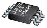
- Packages offered: TSSOP8 and HWSON8