


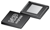

PTN3460IBS是NXP公司的一款高速多路复用器产品,PTN3460IBS是eDP to LVDS bridge for industrial and embedded applications,本站介绍了PTN3460IBS的封装应用图解、特点和优点、功能等,并给出了与PTN3460IBS相关的NXP元器件型号供参考。
PTN3460IBS - eDP to LVDS bridge for industrial and embedded applications - 高速多路复用器 - DisplayPort - 恩智浦, LLC
PTN3460I is an (embedded) DisplayPort to LVDS bridge device that enables connectivitybetween an (embedded) DisplayPort (eDP) source and LVDS display panel. It processesthe incoming DisplayPort (DP) stream, performs DP to LVDS protocol conversion andtransmits processed stream in LVDS format.
PTN3460I has two high-speed ports: Receive port facing DP Source (for example,CPU/GPU/chip set), Transmit port facing the LVDS receiver (for example, LVDS displaypanel controller). The PTN3460I can receive DP stream at link rate 1.62 Gbit/s or2.7 Gbit/s and it can support 1-lane or 2-lane DP operation. It interacts with DP source viaDP Auxiliary (AUX) channel transactions for DP link training and setup.
It supports single bus or dual bus LVDS signaling with color depths of 18 bits per pixel or24 bits per pixel and pixel clock frequency up to 112 MHz. The LVDS data packing can bedone either in VESA or JEIDA format. Also, the DP AUX interface transportsI2C-over-AUX commands and support EDID-DDC communication with LVDS panel. Tosupport panels without EDID ROM, the PTN3460I can emulate EDID ROM behavioravoiding specific changes in system video BIOS.
PTN3460I is suitable for industrial design due to its wide temperature range of -40 °C to+85 °C.
PTN3460I provides high flexibility to optimally fit under different platform environments. Itsupports three configuration options: multi-level configuration pins, DP AUX interface, andI2C-bus interface.
PTN3460I can be powered by either 3.3 V supply only or dual supplies (3.3 V/1.8 V) andis available in the HVQFN56 7 mm x 7 mm package with 0.4 mm pitch.
Device features
- Embedded microcontroller and on-chip Non-Volatile Memory (NVM) allow for flexibilityin firmware updates
- LVDS panel power-up (/down) sequencing control
- Firmware controlled panel power-up (/down) sequence timing parameters
- No external timing reference needed
- EDID ROM emulation to support panels with no EDID ROM. Emulation ON/OFF is setvia configuration pin CFG4:
- Supports EDID structure v1.3
- On-chip EDID emulation up to seven different EDID data structures
- eDP complying PWM signal generation or PWM signal pass through from eDP source
DisplayPort receiver features
- Compliant to DP v1.2a and v1.1a
- Compliant to eDP v1.2 and v1.1
- Supports Main Link operation with one or two lanes (select through configuration pinCFG3)
- Supports Main Link rate: Reduced Bit Rate (1.62 Gbit/s) and High Bit Rate (2.7 Gbit/s)
- Supports 1 Mbit/s AUX channel:
- Supports Native AUX and I2C-over-AUX transactions
- Supports down spreading to minimize EMI
- Integrated 50 Ω termination resistors provide impedance matching on both Main Linklanes and AUX channel
- High performance Auto Receive Equalization enabling optimal channel compensation,device placement flexibility and power saving at CPU/GPU
- Supports eDP authentication options: Alternate Scrambler Seed Reset (ASSR) andAlternate Framing
- Supports Full Link training
- Supports DisplayPort symbol error rate measurements
- Supports PCB routing flexibility by programming for:
- AUX P/N swapping
- DP Main Link P/N swapping
LVDS transmitter features
- Compatible with ANSI/TIA/EIA-644-A-2001 standard
- Supports RGB data packing as per JEIDA and VESA data formats
- Supports pixel clock frequency from 6 MHz to 112 MHz
- Supports single LVDS bus operation up to 112 mega pixels per second
- Supports dual LVDS bus operation up to 224 mega pixels per second
- Supports color depth options: 18 bpp, 24 bpp
- Programmable center spreading of pixel clock frequency to minimize EMI
- Supports 1920 x 1200 at 60 Hz resolution in dual LVDS bus mode
- Programmable LVDS signal swing to pre-compensate for channel attenuation or allowfor power saving
- Supports PCB routing flexibility by programming for:
- LVDS bus swapping
- Channel swapping
- Differential signal pair swapping
- Supports Data Enable polarity programming
- DDC control for EDID ROM access; I2C-bus interface up to 400 kbit/s
Control and system features
- Device programmability:
- Multi-level configuration pins enabling wider choice
- I2C-bus slave interface supporting Standard-mode (100 kbit/s) andFast-mode (400 kbit/s)
- Power management:
- Low-power state: DP AUX command-based Low-power mode (SET POWER)
- Deep power-saving state via a dedicated pin
General
- Power supply: with on-chip regulator
- 3.3 V ±10 % (integrated regulator switched on)
- 3.3 V ±10 %, 1.8 V ±5 % (integrated regulator switched off)
- ESD: 8 kV HBM, 1 kV CDM
- Operating temperature range: -40 °C to +85 °C
- HVQFN56 package 7 mm x 7 mm, 0.4 mm pitch; exposed center pad for thermal reliefand electrical ground
- Industrial PC design
- Printer display
- Automotive dashboard display
- AIO platforms
- Notebook platforms
- Netbooks/net tops